選択した通貨は参考です。お支払いはUSドルで行ってください。
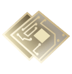
FR-4は、リジッドPCB用の最も一般的な基板材料です。
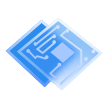
フレキシブルPCBは、薄く柔軟なポリマーフィルムを回路基板として利用します。フレキシブルPCBはスペースの消費を減らし、重量を軽くします。
アルミ/銅コア基板は、標準的なFR-4構造よりも放熱性と熱伝導性に優れています。
注意:アルミ/銅コア基板の場合、最小ドリルサイズは1.0mm、最小スロット幅は1.6mmです。
ロジャース/テフロンPCBは、優れた誘電特性と最小限の抵抗を持っています。一般的に高速、高周波回路用途に使用されます。
詳細はこちら
最大20層、インピーダンス制御、高速ターンリジッドPCB、比較的低コスト。
優れた柔軟性、スペースと重量の削減、高密度化、エラーの最小化。
熱伝導性、電気絶縁性に優れ、LED用途に適しています。
高熱伝導性と放熱性、高出力電源、LEDアプリケーション。
低誘電正接、固体寸法安定性、高周波用途。
より低い損失係数、高温および高周波アプリケーション。
The number of copper layers in your PCB is defined as its layer count. A PCB with a single copper layer is termed a 1-layer PCB.
注意:
1. A 1-layer PCB typically features solder mask on one side only. For solder mask on both sides, please order a 2-layer PCB.
2. For PCB designs with an odd layer count, such as 3 or 5 layers, fabrication will be adjusted to the next even layer count, i.e., 4 or 6 layers. Please select the appropriate even layer count when placing your order.
アップロードする面付けなしまたはPCB面付けの寸法。
No data
This is the number of single boards or panels you require.
For single-board designs, it is the number of single boards. For panelized designs, it is the number of panels. If you choose "Panel by JLCPCB", it is also the number of panels.
1. Choose from the available quantities on our website; custom quantities like 3pcs or 8pcs are not supported. If you need more than the maximum quantity offered on the website, please contact our support team for assistance.
2. For orders over 200 pieces, we advise prototyping your PCBs before starting small-batch production.
航空宇宙産業と医療産業では、すべてのユーザーの安全と安心を確保するために、厳しい製品要件が維持されています。製品の品質を保証するために、航空宇宙および医療製品では以下のオプションを選択する必要があります。
1. 2層のボードの場合、「4-Wire Kelvin Test」オプションが必要です。
2. 4層および6層のボードの場合、「4-Wire Kelvin Test」と「FR4 Tg155」オプションが必要です。
3. 8層以上のボードの場合、「4-Wire Kelvin Test」オプションが必要です。
Vカット、マウスバイト、ミリングスロットで区切られたファイルに、いくつの異なるデザインがありますか?例えば:
配達形式とは、お客様がJLCPCBにPCBデザインの製作と納品を依頼する方法です。
· 面付けなし - 現状のままのデザインです。
· 面付け済み - 顧客自身がPCBパネルを構築し、パネル化されたデータを提供します。
· JLCPCBによる面付け - 必要に応じてVカットでパネルを構築します。(長方形や円などの定型形状のPCBに対してのみパネル化サービスを提供しています。不規則な形状のPCBの場合は、自分でパネル化する必要があります。)
完成した基板の厚み。基板の厚みの許容誤差は+/-10%です。
1. For boards with a 0.40 mm thickness, we only accept an ENIG finish. These cannot be made with a panel and are not available for 1-layer PCBs.
2. For boards with a 0.60 mm thickness, the maximum PCB size is 100 mm x 100 mm. This thickness is not available for 1-layer, 4-layer, or 6-layer PCBs.
3. For boards with a 0.8 mm to 1.0 mm thickness, the maximum PCB size is 300 mm x 300 mm.
The PCB solder mask color. Solder mask is used to protect the copper traces of the PCB and ensures that the solder will only flow on the exposed pads.
The green standard has the best performance and fastest turnaround time. For most colors, the silkscreen is printed white. Only for white solder mask, the silkscreen is printed black.
ほとんどの色では、シルクスクリーンは白で印刷されます。白いはんだマスクの場合のみ、シルクスクリーンは黒で印刷されます。ただし、白い印刷されたシルクスクリーンは灰色の表面と混ざりやすいことにご注意ください。裸のアルミニウム表面にはシルクスクリーンはおすすめしません。 詳細はこちら
HASLは、PCB上に薄い保護カバーを作成するために錫/鉛を利用する手頃な価格の仕上げオプションです。
ENIGは、フラットな表面、無鉛およびRoHS準拠、長い保存期間、およびプレートホールのためのより狭い許容差を提供することから、業界で最も人気のある表面仕上げとなっています。 詳細はこちら
外層(上下)に銅のウェイト。
内層の銅の重さはデフォルトで0.5オンス。 詳細はこちら
最小ビア径/ランド径
ビア径は、ビアホールのサイズより0.1mm(0.15mmが望ましい)大きいこと。
例:ビアホールのサイズが0.2mmの場合、ビア径は0.3mmまたは0.35mmとする
お知らせ: ビアホール<0.3mm、ビア径≦0.4mmの場合、追加料金がかかります。ビアホール<0.3mm、ビア径>0.4mmの場合、追加料金はかかりません。
例:0.2mm穴/0.4mm径は追加料金が必要ですが、0.2mm穴/0.45mm径は無料です。
お客様のPCBを簡単に識別し、他のPCBと混同しないように、JLCPCBはお客様のPCBに注文番号を割り当てます。
注文番号を特定の位置に付けたい場合は、「注文番号(位置指定)」オプションを選択し、シルクスクリーン層に「JLCJLCJLCJLC」というテキストを追加して、この位置を示してください。
PCBのトレーサビリティを強化するために、各PCBに2次元バーコードのシリアル番号を適用するオプションもあります。 このオプションを選択すれば、注文番号が削除されます。
注文番号、二次元バーコード(シリアル番号)を含むマークの削除をご希望の場合は、下記の「マークを削除する」をご選択ください。なお、1層から6層までは無料、8層以上は有料となります。
このサービスはカスタマイズ可能ですので、「製造用ファイルの事前確認」オプションを選択することをお勧めします。
JLCPCBでは、すべてのPCBは、品質を確保するために包括的なAOI(自動光学検査)を受けています。AOIはトレースの断線や欠陥を検出します。AOIで検査されたPCBは99%以上の品質率を達成しています。
フライング・プローブテスト: これは回路の連続性を確認する最終チェックポイントです。開回路や短絡を検出できます。
- フルテスト:100%の合格率を保証しますが、時間がかかり、そのため費用が発生します。
- ランダムテスト:無料で行われ、99%以上の合格率を保証します。
Eテスト治具: 迅速なテストが可能で、大量生産に適していますが、高い材料費がかかります。
金端子とは、プリント基板の接続端に沿って金メッキされた柱のことです。ENIG表面仕上げを選択した場合のみ、端子に金メッキが施されます。HASL表面仕上げを選択した場合、エッジコネクトメッキとしてHASLを使用します。 詳細はこちら
キャステレーションは、プリント基板の端にあるスルーホールにメッキを施したもので、半穴が連なるように切り抜かれている。
端面スルーホールの最小直径は0.5mm。 詳細はこちら
ビルド時間は、物理的な生産の開始("生産進捗状況 "でMIが開始されたとき)から生産完了(配信準備完了)までの期間を指します。


 Welcome back, may I help you?