選擇產品
標準 PCB/PCBA
進階 PCB/PCBA
SMT 鋼網
柔性加熱器
機電一體化零件
3D 列印
CNC 加工
印刷電路板佈局
鈑金
FR-4 是剛性 PCB 最常用的基板材料。
軟板PCB 利用薄而柔軟的聚合物薄膜作為電路基板。軟板 PCB 可減少空間消耗,重量也較輕。
與標準 FR-4 結構相比,鋁/銅芯板具有更好的散熱性和熱傳導性。
注意:對於鋁/銅芯板,最小鑽孔尺寸為 1.0mm,最小槽寬為 1.6mm。
Rogers/Teflon PCB 具有優異的介電特性和最小的電阻。它們通常用於高速、高頻電路應用。
瞭解更多
多達 20 層、控制阻抗、快速轉換剛性 PCB、相對較低的成本。
良好的彈性、減少空間與重量、更高的密度、最小化誤差。
良好的導熱性與電絕緣特性、LED 應用。
高導熱性與散熱性、大功率電源與 LED 應用。
低損耗因素、堅固的尺寸穩定性、高頻應用。
低損耗因素,高溫高頻應用。
PCB 板的銅層數量定義為其層數。單層銅板稱為單層 PCB。
注意事項:
1. 單層PCB通常僅一面有阻焊層。如需雙面都帶有阻焊層,請訂購雙層PCB。
2. 對於奇數層(例如3層或5層)的PCB設計,生產將調整為下一個偶數層(例如4層或6層)。請在下單時選擇合適的偶數圖層。
您上傳的單一 PCB 或 PCB 拼板的尺寸。
無資料
這是您需要的單板或拼板的數量。
對於單板設計,此值指的是單板數量。對於拼板設計,此值指的是拼板數量。如果您選擇“JLCPCB 拼板”,此數值也指的是拼板數量。
1. 請從我們網站上的可用數量中選擇;不支持 3 件或 8 件等自訂數量。如果您需要的數量超過網站上提供的最大數量,請聯絡我們的支援團隊尋求協助。
2. 對於超過 200 件的訂單,我們建議在開始小批量生產之前先製作 PCB樣板。
在航空與醫療產業中,對產品有嚴格的要求,以確保所有使用者的安全與保障。為了確保產品品質,航空和醫療產品需要選擇以下選項。
1. 對於 2 層板,需要選擇 「4-Wire Kelvin Test 」選項。
2. 對於 4 層和 6 層板,需要選擇 「4-Wire Kelvin Test 「和 」FR4 Tg155 」選項。
3. 對於 8 層以上的電路板,需要 「4-Wire Kelvin Test」 選項。
在您的檔案中,有多少不同的設計是以 V 形切割、郵票孔或鑼槽來分隔。舉例來說:
交貨形式是指您要求 JLCPCB 製作和交付您的 PCB 設計的方式。
· 單層PCB - 您的設計原樣。
· 客戶提供拼板 - 您自行建構 PCB 拼板,並提供給我們 PCB 生產的拼板資料。
· JLCPCB提供拼板 - 我們根據您的需求,以V-cut方式製作您的拼板。(我們只提供矩形和圓形等規則形狀 PCB 的拼板化服務。對於不規則形狀的 PCB,您需要自行製作拼板)。
成品板的厚度。板厚公差為+/-10%。
1. 對於厚度為 0.40 mm的電路板,我們僅接受沉金 (ENIG) 處理。此類電路板無法使用拼板工藝,不適用於單層 PCB。
2. 對於厚度為 0.60 mm的電路板,最大 PCB 尺寸為 100 mm x 100 mm。此厚度不適用於 1 層、4 層或 6 層 PCB。
3. 對於厚度0.8mm至1.0mm的電路板,最大的PCB尺寸為300mmx30mm。
PCB 阻焊層顏色。阻焊層用於保護 PCB 的銅走線,並確保焊料僅流過裸露的焊盤。
綠色標準性能最佳,生產周期最快。大多數顏色的絲印為白色。只有白色阻焊層絲印是黑色。
3.對於大多數的顏色,絲印是印白色的。僅對於白色阻焊層,絲印為黑色。請注意,白色印刷的絲印很容易與灰色表面混淆。不建議在裸露的鋁表面上進行絲印。 瞭解更多
HASL 是一種經濟實惠的表面處理選項,利用錫/鉛在 PCB 上形成薄薄的保護層。
ENIG 已成為業界最受歡迎的表面處理方式,因為它具有平坦的表面、無鉛且符合 RoHS 標準、保質期更長、鍍孔公差更嚴格等特點。 瞭解更多
外層(頂層和底層)的銅重。
內層的銅重默認為 0.5 oz。 瞭解更多
對於 1/3 oz和 0.5 oz,覆蓋層為 12.5 μm,膠水為 15 μm。
對於1oz銅,覆蓋層為25μm,膠水為25μm。
裸露 FPC 非常輕且柔軟。當安裝或組裝時需要 FPC 的厚度或強度時,可以在板的表面附加一層剛性材料。這種剛性材料稱為補強。
1. 我們提供聚醯亞胺、FR4、不銹鋼及 3M 膠帶等補強材料。
2.不同厚度和材質的補強可以用在相同的 FPC 上。
3.「補強厚度 」僅指硬片。總厚度是此值加上 FPC 的厚度。
4. 必須與其他設計檔案一起提供圖面或額外的 Gerber 圖層,以顯示補強的位置、材質和厚度。預期格式請參閱圖表。
對於金手指,如果需要,請務必增加補強,使連接器有足夠的強度與插座接合。
柔性電路板由於體積小且缺乏遮蔽,因此容易受到電磁干擾 (EMI),EMI 遮蔽膜有助於降低電磁干擾,以解決 EMI 問題。此薄膜可應用於 FPC 的兩面或僅一面(請在設計檔案中說明是哪一面)。
默認方式是雷射切割。切割邊緣的碳化會導致電路板輪廓輕微收縮。為了防止金手指下方的支撐被移除,在我們的 DFM 製程中,所有金手指都會被縮短 0.2 mm。
最小過孔尺寸和過孔直徑。
過孔直徑應比過孔尺寸大 0.1mm(優先選擇 0.15mm)。
例如:當過孔尺寸為 0.2mm 時,過孔直徑應為 0.3mm 或 0.35mm。
注意事項: 當過孔<0.3mm且過孔直徑≤0.4mm時,將收取額外費用。過孔≥0.3mm,且過孔直徑≥0.4mm時,不另收費。
「如0.2mm孔徑/0.4mm直徑需額外收費,而0.3mm孔徑/0.40mm直徑免費。
預設不會新增任何標記。為提升 PCB 的可追溯性,您可以選擇「二維條碼(序號)」選項。
我們可僅列印二維條碼、僅列印序號,或同時列印二維條碼與序號。
如需將二維條碼或序號放置於指定位置,請在您的絲印層加入實心方塊:二維條碼請依其尺寸(5×5 mm、8×8 mm 或 10×10 mm)放置相同尺寸的實心方塊;若僅列印序號,請放置 2×10 mm 的實心方塊,並在二維條碼選項中選擇「指定位置」。
新增二維條碼(序號)不收取服務費。不過,由於此服務可客製化,建議您選擇「確認生產檔案」選項,以免發生錯誤。
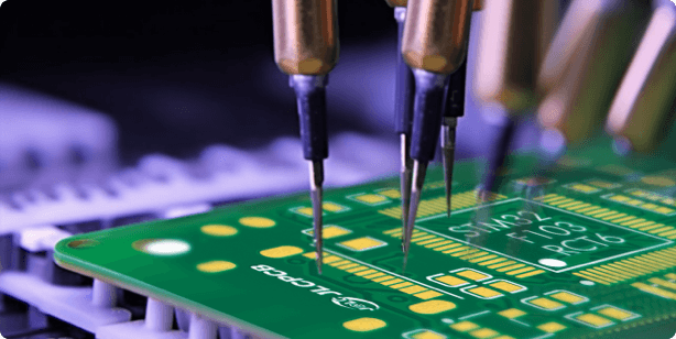
在 JLCPCB,所有的 PCB 都會經過全面的 AOI(自動光學檢查),以確保品質。AOI 可以檢測到跡線中的任何斷裂或瑕疵。經 AOI 檢測的 PCB 品質達到 99% 以上。
飛針測試: 這是電路連續性的最後檢查點。它可以測試開路和短路。
- 全面測試:100% 合格率,但速度較慢,且因耗費時間而需要收費。
- 隨機測試: 免費,確保最低 99% 的合格率。
E-test 治具: 提供快速測試,適合大量生產,但需要較高的材料成本。
金手指是沿 PCB 連接邊緣鍍金。只有選擇 ENIG 表面處理時,金手指才會鍍金。如果您選擇 HASL 表面處理,我們會使用 HASL 來電鍍邊緣。 瞭解更多
Castellations 是位於印刷電路板邊緣的電鍍通孔,切割後形成一系列的半孔。
半孔的最小直徑為 0.5mm。 瞭解更多
製造時間是指從實體生產開始(MI 在 「生產進度 」中開始)到生產完成(準備發送到出貨中心)的時間。